Via Covering means that the via is covered by a solder mask or other chemical materials. Why do I sometimes need to cover vias during PCB manufacturing? Because if the through hole is exposed, solder paste may enter the through hole and cause poor solder joints or short circuits. The situation where the via is not covered is called a via opening.
The Seven Common Types Of PCB Via Coverage.
Production-related requirements of PCB manufacturing or several technologies require via protection, so the via fill can be very important to your PCB. In general, these types of via coverage are possible:
Simple Coverage: Via Tent or Tent Vias
Partial Fill: Via Plugging or Plugged Vias
Fully Filled: Via Filling or Filled Vias
But sometimes designers don’t fully understand all the available via coverage types and which ones to specify. Rather than confuse designers and manufacturers by simply specifying that vias must be “plugged” or “filled,” we recommend specifying specific IPC-4761 via type. This helps to make it easier for designers and manufacturers to understand. IPC-4761 specifies only mechanically drilled via types, not laser-drilled micro vias. Learn more about the types of PCB through holes.
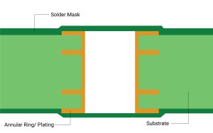
What Is A Tented Vias?
Via tented refers to covering the vias and annular rings with solder mask, that is, creating a shape like tent over the opening to hide the vias. A via is a hole comes from a PCB that allows signals connect from one layer to another on the PCB. Vias are generally copper-plated, so this material is strongly conductive. The main purpose of tenting vias is to reduce the number of exposed conductive pads on the PCB and decrease unexpected short circuit or touch circuits. So far, tented via is the most developed and prevalent process in PCB manufacture. Via tenting means that the through hole is only covered by solder mask ink . This is the easiest way of Via Covering. No additional process steps are required in the manufacturing process. Generally, vias using this type of coverage should not be larger than 0.3mm.
What Is A QFP Package?
QFP (Quad Flat Package) is a quad flat package, a surface mount package with pins leading from all four sides in a seagull wing (L) shape. It is very popular in Quad Flat Packs. The reason is that the finely etched or stamped lead frame allows the QFP to contain more leads and have a smaller profile to achieve better electrical characteristics with shorter interconnects (lead widths as small as 0.16mm and outer lead spacing as small as 0.35 mm to 1.27 mm). The thinner, more flexible gull-wing leads also provide better secondary reliability (package-to-PCB reliability). All four sides are gull-wing (L) shaped. It is popular in four-sided flat packages. The reason is that finely etched or stamped leadframes allow QFPs to contain more leads and have a smaller profile for better electrical characteristics with shorter interconnects. Thinner, more flexible gull-wing leads also provide better secondary reliability (package-to-PCB reliability). Generally large scale or ultra-large scale ICs are packaged in this package form and their pin count is typically 100 or more. Its smaller package size and lower parasitic parameters make it suitable for high-frequency applications; the technology is primarily suitable for mounting wiring on PCBs using SMT surface mount technology. Of course, there are many other different PCB package types at JHD to meet different conditions.
QFP package has the following features:
The ease of operation and high reliability of the technology when packaging CPUs.
Its smaller package form factor and reduced parasitic parameters, making it suitable for high frequency applications.
The technology is primarily suitable for mounting wiring on PCBs using SMT surface mount technology.
Substrates For QFP Packaging Technology.
The substrates for QFP packaging technology are ceramic, metal and plastic. By volume, plastic packages make up the majority. When no material is specified, the plastic QFP is the most popular multi-pin LSI package. It is utilized for analog LSI circuits like VTR signal processing and audio signal processing in addition to digital logic LSI circuits like microprocessors and gate displays.
The pin center spacing is 1.0 mm, 0.8 mm, O.65 mm, 0.5 mm, 0.4 mm, 0.3 mm, etc. The maximum number of pins in the 0.65 mm center pitch specification is 304. Profile Quad Flat Package (1.4 mm thick) and Thin Quad Flat Package (TQmin Quad Flat Package, 1.0 mm thick). In addition, some LSI manufacturers refer to QFPs with 0.5 mm pin centers as Shrink QFPs or SQFPs or VQFPs, while others refer to QFPs with 0.65 mm and 0.4 mm pin centers as SQFPs. In the logic LSI field, many development and high-reliability products are available in multilayer ceramic QFP packages. Products with a minimum pin center distance of 0.4 mm and a maximum pin count of 348 pins are also available. The disadvantage of the QFP package is that the pins tend to bend when the pin center distance is less than 0.65 mm. To prevent pin distortion, several improved QFP variants have emerged.